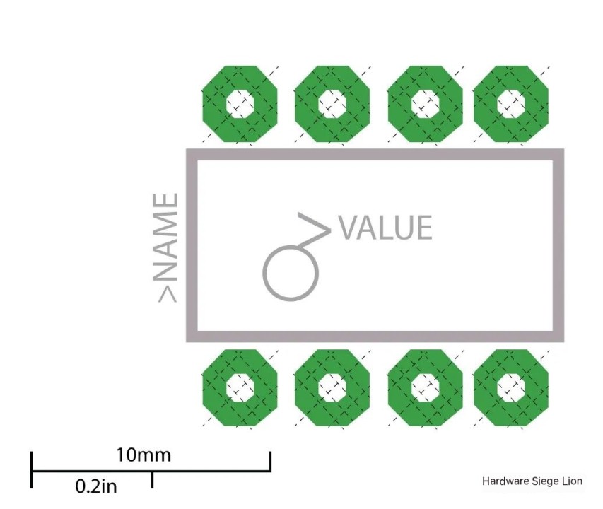
What is a Pad in PCB Design? Essential Guide for Developers What is a pad in pcb design and development
If you are looking for PCB Pad Fundamentals: Concepts, Types, and Design Guidelines - TechSparks you've came to the right web. We have 25 Pictures about PCB Pad Fundamentals: Concepts, Types, and Design Guidelines - TechSparks like PCB design in the shape and size of the pad design standards | Andwin, PCB - Design Guidlines PDF | PDF | Electronic Component | Printed and also The Pad Design Of PCB Components - 86PCB. Here it is:
PCB Pad Fundamentals: Concepts, Types, And Design Guidelines - TechSparks
 www.tech-sparks.com
PCB Pad Fundamentals: Concepts, Types, and Design Guidelines - TechSparks
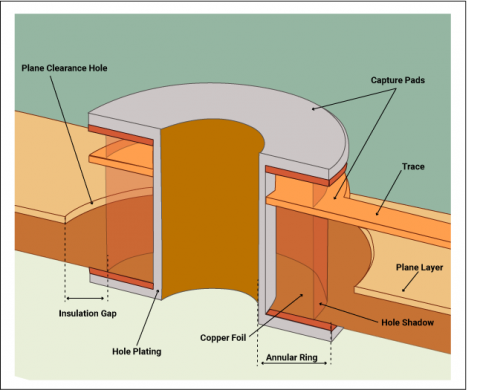
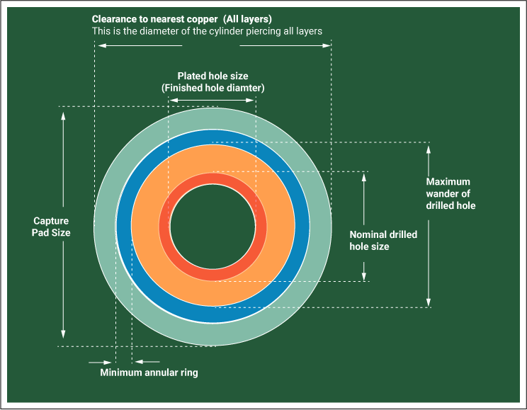
PCB Design Pad Types And Design Criteria
 support.wonderfulpcb.com
PCB Design Pad Types and Design Criteria
Siemens PCB Schematic Design | PADS Professional | Cadlog
 www.cadlog.com
Siemens PCB Schematic Design | PADS Professional | Cadlog
The Pad Design Of PCB Components - 86PCB
 86pcb.com
The Pad Design Of PCB Components - 86PCB
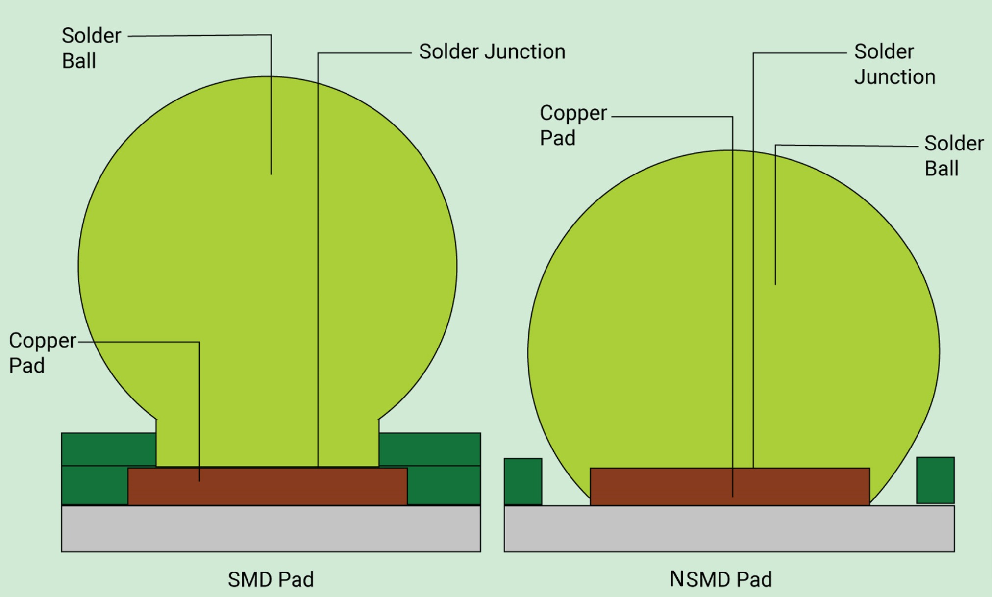
What Is A Pad In PCB Design And Development | Sierra Circuits
 www.protoexpress.com
What is a Pad in PCB Design and Development | Sierra Circuits
PADS PCB Design Software – Krishwave
 krishwave.com
PADS PCB Design Software – krishwave
PCB Layout Design By Siemens | PADS Professional | Cadlog
 www.cadlog.com
PCB Layout Design by Siemens | PADS Professional | Cadlog
What Is A Pad In PCB Design And Development | Sierra Circuits
 www.protoexpress.com
What is a Pad in PCB Design and Development | Sierra Circuits
PCB - Design Guidlines PDF | PDF | Electronic Component | Printed
 www.scribd.com
PCB - Design Guidlines PDF | PDF | Electronic Component | Printed ...
Basic Principles Of PCB Pad Design
 support.wonderfulpcb.com
Basic principles of PCB pad design
PCB Design Guidelines - PCB Online S.r.l
 www.pcbdirectlab.com
PCB design guidelines - PCB Online s.r.l
What Is A Pad In PCB Design And Development | Sierra Circuits
 www.protoexpress.com
What is a Pad in PCB Design and Development | Sierra Circuits
What Is A Pad In PCB Design And Development | Sierra Circuits
 www.protoexpress.com
What is a Pad in PCB Design and Development | Sierra Circuits
PCB Pad – A Basic Guide For Beginners - Mainpcba One-stop PCB Assembly
 www.mainpcba.com
PCB pad – a basic guide for beginners - Mainpcba One-stop PCB Assembly ...
PCB Layout Design By Siemens | PADS Professional | Cadlog
 www.cadlog.com
PCB Layout Design by Siemens | PADS Professional | Cadlog
What Is A PCB Pad - Different Types And Design Guidelines - PCBA
 www.pcba-manufacturers.com
What is a PCB pad - different types and design guidelines - PCBA ...
What Is A Pad In PCB Design And Development? - AES
 absolutepcbassembly.com
What is a Pad in PCB Design and Development? - AES
PCB Pad – A Basic Guide For Beginners - Mainpcba One-stop PCB Assembly
 www.mainpcba.com
PCB pad – a basic guide for beginners - Mainpcba One-stop PCB Assembly ...
What Is A PCB Pad - Different Types And Design Guidelines - PCBA
 www.pcba-manufacturers.com
What is a PCB pad - different types and design guidelines - PCBA ...
PCB Design In The Shape And Size Of The Pad Design Standards | Andwin
 www.andwinpcb.com
PCB design in the shape and size of the pad design standards | Andwin ...
PCB Pad Design Principles And Solderability Issues
 www.linkedin.com
PCB Pad Design Principles and Solderability Issues
What Is A Pad In PCB Design And Development | Sierra Circuits
 www.protoexpress.com
What is a Pad in PCB Design and Development | Sierra Circuits
What Is A Pad In PCB Design? - JHYPCB
 www.pcbelec.com
What is a Pad in PCB Design? - JHYPCB
Day1 Basics Of PCB Design In PADS | PDF | Printed Circuit Board | Design
 www.scribd.com
Day1 Basics of PCB Design in PADS | PDF | Printed Circuit Board | Design
PCB Pad Design Principles
 www.linkedin.com
PCB pad design principles
The pad design of pcb components. what is a pad in pcb design and development. Siemens pcb schematic design